

Omron unveils AI chip inspection tools at SEMICON Taiwan
Tue, 25th Aug 2026.webp)
Omron is presenting semiconductor manufacturing inspection and automation systems at SEMICON Taiwan 2026, with a display focused on quality visualisation in advanced packaging.
Its line-up includes 3D-CT X-ray inspection equipment, digital twin technology and quality data applications for semiconductor and electronic component manufacturing. The systems are positioned across the production cycle, from research and prototype evaluation to volume manufacturing.
The announcement reflects a broader shift in chip production as manufacturers look beyond identifying defective parts and seek to trace faults earlier in the process. Rising complexity in AI-related chips, high-performance computing devices and advanced packaging has increased interest in tools that can inspect internal structures and link those findings to process control.
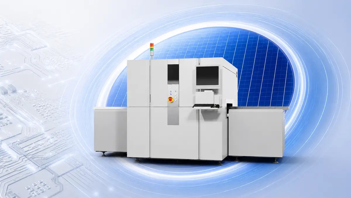
One of the main systems on show is a CT-based 3D X-ray automated inspection setup for advanced packaging. The equipment is designed to inspect through-glass vias, microbumps, voids and chiplets, all of which have become more important as chipmakers stack and connect more components inside a package.
The system combines automated X-ray inspection with CT-based 3D X-ray imaging. In development, it allows engineers to study internal structures in detail. In mass production, it is intended to support more consistent pass-fail decisions on parts moving through the line.
Inspection equipment has become more prominent in back-end semiconductor manufacturing as packaging methods grow more intricate. Defects in bonding, warpage and internal voids can be difficult to detect with conventional surface inspection alone, pushing manufacturers towards volumetric imaging and more data-intensive analysis.
Data focus
Omron is also linking inspection results to digital twin work through its collaboration with Nvidia Omniverse. It is developing digital twins that use quality data generated by visual and X-ray inspections to recreate issues such as substrate warpage and bonding conditions.
The approach is intended to let manufacturers simulate quality conditions in a virtual environment rather than rely only on physical inspection and post-process analysis. By combining imaging data with AI models, the system is designed to connect inspection results more directly with process changes on the factory floor.
The use of digital twins in semiconductor manufacturing has expanded in recent years as companies seek to model equipment, materials and process conditions before making production adjustments. In packaging, where multiple process steps can affect final yield, a digital replica can help engineers isolate how a defect emerges and whether it is tied to material variation, machine settings or handling conditions.
Omron said the visualisation generated through visual and X-ray inspection can reproduce quality conditions with greater accuracy. That could be useful when warpage or bonding problems are intermittent and hard to capture consistently through manual checks.
Factory systems
Alongside inspection and simulation tools, Omron is showing wafer-handling technologies, visual inspection systems and control products for semiconductor manufacturing. It is also highlighting safety and sensor technology developed at its semiconductor development centre.
Material handling remains a significant issue in semiconductor plants because wafers, substrates and packaged devices move through tightly controlled processes where contamination, positioning errors and mechanical stress can lead to yield losses. Suppliers of automation equipment have sought to integrate handling, sensing and inspection more closely so process data can be fed back into production decisions.
Founded in 1933, Omron operates across industrial automation, healthcare, social systems, and devices and module solutions. It says it has about 27,000 employees worldwide and sells products and services in more than 130 countries.
The semiconductor segment has become an important test case for industrial automation suppliers because chip factories demand high levels of repeatability, traceability and process monitoring. As manufacturers increase investment in advanced packaging to meet demand from AI and computing markets, suppliers of inspection and production control systems are trying to show that manufacturing data can do more than flag errors after they appear.
Omron's exhibition concept is built around "Enhancing AI Manufacturing Through Quality Visualization".